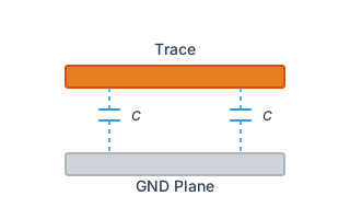
PCB design calculators
Online calculators that run in your browser, aimed at hardware and PCB engineers. They cover characteristic impedance, propagation delay, trace resistance and parasitics. Some fields accept SI prefixes (k, M, G, u, n, p).
TOOL Circuit simulators in your browser — build a circuit and watch the waveforms with CircuitJS1, or run an IBIS model through a PCB trace.
Propagetion velocity on pcb
This is a calculator for the propagation speed of radio waves on a substrate. The higher the dielectric constant, the lower the propagation speed. Substrates with a low dielectric constant have the advantage of low propagation delay for high-speed signals (such as 5G and millimeter wave).
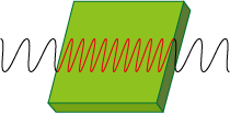
Pattern resistance, heat generation, inductance, parasitic capacitance
This is a calculator for pattern resistance, pattern heat generation, pattern inductance and parasitic capacitance. Resistance and inductance (inductance) components are also generated in the copper foil pattern of the board. Patterns with large currents and high-speed signals where inductance is a concern should be treated with caution. Guidelines for copper foil thickness: 35um on the surface layer of a rigid board, 12um on the surface layer of a flexible board .

SI prefixes accepted (4k7 / 1M / 10m / 220). Upper-case M = mega, lower-case m = milli
Advanced — Dielectric thickness, Pcb relative permittivity
Derived values
- Voltage drop
- 33.143 mV
- Current × trace resistance
Via and through-hole inductance
This is a calculator for via inductance, parasitic capacitance and circumference. Inductive and capacitive components are also generated in through-hole vias for pattern wiring. The circumference of the via should be used as a guide to how much pattern width the via corresponds to.

Advanced — Clearance hole diametor, Pcb relative permittivity
Skin effect
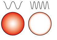
This is a calculator for the depth at which the current decays to 1/e=0.37 times the surface of the conductor. A signal propagating through a conductor tends to flow more easily on the surface of the conductor and less easily on the inside. The higher the frequency of the signal, the stronger the tendency. Impulse noise and electrostatic noise have higher frequencies and tend to flow more easily to the surface of the conductor or board due to the skin effect.
SI prefixes accepted (4k7 / 1M / 10m / 220). Upper-case M = mega, lower-case m = milli
Characteristic impedance
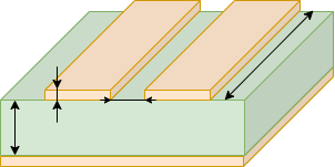
This is a calculator for the characteristic impedance of surface wiring. For high-speed signals, surface mount wiring with low effective dielectric constant (i.e., low loss and delay) is recommended. Single 50Ω: DDR data bus, DDR address bus Differential 75Ω: Analog video signal Differential 85Ω: USB, PCI Express Differential 90Ω: DDR DQS, DDR clock Differential 100Ω: Ether, MDII, LVDS, MIPI
SI prefixes accepted (4k7 / 1M / 10m / 220). Upper-case M = mega, lower-case m = milli
Advanced — Cu thickness, Pcb relative permittivity
Derived values
- Effective permittivity εeff
- 2.71
- 0.475 × εr + 0.67
- Propagation delay
- 5.49 ps/mm
- Used for length matching
- Capacitance per length
- 0.112 pF/mm
- TD / Z0
- Inductance per length
- 0.27 nH/mm
- TD × Z0
A 1 ns skew corresponds to 182 mm of trace length (length matching rule of thumb).
Allowing the usual ±10% fabrication tolerance, the single-ended value lands between 44.22 and 54.04 Ω.
Concentration and distribution constant
This is a calculator for the borderline between a concentration constant and a distribution constant. By inputting the frequency, it will find the limit wiring length that can be treated as a concentration constant. When the wiring length is input, the limit frequency that can be treated as a concentration constant is obtained .

SI prefixes accepted (4k7 / 1M / 10m / 220). Upper-case M = mega, lower-case m = milli
Advanced — Dielectric thickness, Cu thickness, PCB relative permittivity
Convert delay time to line length
It is calculated by converting the delay time ps into the pattern length (= distance). Inner layer pattern length: so-called strip line. It is determined by the dielectric constant of the substrate. Surface layer pattern length: so-called microstrip line. In addition to the dielectric constant of the substrate, it is also affected by the line width and the thickness of the dielectric.
PCB weight
Calculator for the weight of a printed circuit board. Estimates the board mass from its outer dimensions. The FR-4 substrate and the copper foil are shown separately.
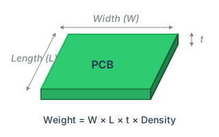
Advanced — Density of copper, Density of substrate
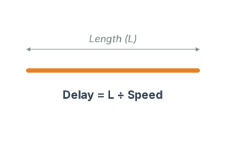
Convert line length to delay time
Pattern length to propagation delay conversion Reverse calculation of delay time
Trace capacitance
Trace capacitance calculation Capacitance component of transmission lines (Stripline)