Convert line length to delay time
Pattern length to propagation delay conversion Reverse calculation of delay time
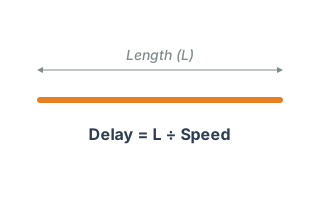
mm
εr
mm
mm
Inner layer delay
6.9ps
Outer layer delay
5.9ps
History
Press Enter in any field to keep a snapshot here.
Formula
Inner layer (stripline): TD = L × √εr / c [ps]
Outer layer (microstrip): TD = L × √εeff / c [ps]
εeff = (εr+1)/2 + (εr-1)/2 × (1+10h/w)^-0.5
Outer layer (microstrip): TD = L × √εeff / c [ps]
εeff = (εr+1)/2 + (εr-1)/2 × (1+10h/w)^-0.5
Design notes
Calculates propagation delay from trace length. This is the basis of length matching and skew control on high-speed interfaces.
DDR-SDRAM example:
• DDR4-3200: one bit period ≈ 313 ps
• Skew budget ≈ ±20 ps, which is about ±1.4 mm of trace length
Working out the allowable length error from the delay budget before setting up length matching constraints in your PCB CAD tool makes the layout go much more smoothly.