It'a REALTIME ONLINE calculator!
Out targets are Hardware, pcb, system engineer
You may use metric Prefixies(like k, m,u,n,p,...).
This is a calculator for the propagation speed of radio waves on a substrate. The higher the dielectric constant, the lower the propagation speed.
Substrates with a low dielectric constant have the advantage of low propagation delay for high-speed signals (such as 5G and millimeter wave). 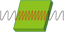
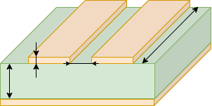
This is a calculator for pattern resistance, pattern heat generation, pattern inductance and parasitic capacitance.
Resistance and inductance (inductance) components are also generated in the copper foil pattern of the board.
Patterns with large currents and high-speed signals where inductance is a concern should be treated with caution.
Guidelines for copper foil thickness: 35um on the surface layer of a rigid board, 12um on the surface layer of a flexible board
.

This is a calculator for via inductance, parasitic capacitance and circumference.
Inductive and capacitive components are also generated in through-hole vias for pattern wiring.
The circumference of the via should be used as a guide to how much pattern width the via corresponds to. 
This is a calculator for the depth at which the current decays to 1/e=0.37 times the surface of the conductor.
A signal propagating through a conductor tends to flow more easily on the surface of the conductor and less easily on the inside.
The higher the frequency of the signal, the stronger the tendency.
Impulse noise and electrostatic noise have higher frequencies and tend to flow more easily to the surface of the conductor or board due to the skin effect. 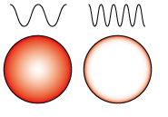
This is a calculator for the characteristic impedance of surface wiring.
For high-speed signals, surface mount wiring with low effective dielectric constant (i.e., low loss and delay) is recommended.
Single 50Ω: DDR data bus, DDR address bus
Differential 75Ω: Analog video signal
Differential 85Ω: USB, PCI Express
Differential 90Ω: DDR DQS, DDR clock
Differential 100Ω: Ether, MDII, LVDS, MIPI
This is a calculator for the borderline between a concentration constant and a distribution constant.
By inputting the frequency, it will find the limit wiring length that can be treated as a concentration constant.
When the wiring length is input, the limit frequency that can be treated as a concentration constant is obtained
.

It is calculated by converting the delay time ps into the pattern length (= distance).
Inner layer pattern length: so-called strip line. It is determined by the dielectric constant of the substrate.
Surface layer pattern length: so-called microstrip line. In addition to the dielectric constant of the substrate, it is also affected by the line width and the thickness of the dielectric.
This is a easy calculation and no guarantee is given for the calculation results.
2020 Engeneer Calculator project.
2020 Engeneer Calculator project. All right reserve.